How is the NAND gate implemented? (Conceptually)
Categories:
Understanding the NAND Gate: A Conceptual Implementation

Explore the fundamental concept of the NAND gate, its truth table, and how it can be conceptually implemented using basic electronic components or logical operations.
The NAND gate, short for 'NOT-AND', is a universal logic gate, meaning any other logic gate (AND, OR, NOT, NOR, XOR, XNOR) can be constructed solely using NAND gates. Understanding its conceptual implementation is crucial for grasping the basics of digital electronics and boolean logic. This article will delve into its truth table, basic circuit representation, and how it functions at a high level.
What is a NAND Gate?
A NAND gate is a digital logic gate that produces an output that is false only if all its inputs are true; otherwise, the output is true. In terms of binary, it outputs 0 only if all inputs are 1, and outputs 1 if any input is 0. This behavior is the inverse of an AND gate. It typically takes two or more binary inputs and produces a single binary output.
flowchart TD
    A[Input A] --> B{AND Operation}
    C[Input B] --> B
    B --> D[NOT Operation]
    D --> E[Output]
Conceptual flow of a NAND gate as an AND followed by a NOT operation
Truth Table of a Two-Input NAND Gate
The truth table defines the output of a logic gate for all possible combinations of its inputs. For a two-input NAND gate, let's consider inputs A and B, and output Q. The table clearly illustrates that the output is only low (0) when both inputs are high (1).
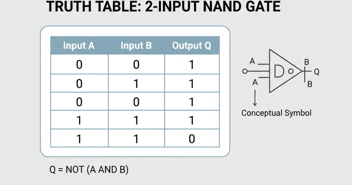
Truth Table for a 2-Input NAND Gate
Conceptual Implementation with Transistors
While modern integrated circuits use complex designs, conceptually, a NAND gate can be built using transistors (e.g., NPN or MOSFETs) and resistors. The most common conceptual model involves two transistors connected in series, followed by an inverter (NOT gate). When both transistors are 'on' (inputs are high), they allow current to flow, pulling the output low. If either transistor is 'off' (any input is low), current cannot flow through both, and the output remains high due to a pull-up resistor.
flowchart LR
    subgraph Inputs
        A[Input A]
        B[Input B]
    end

    subgraph Transistor Logic
        A --> T1(Transistor 1)
        B --> T2(Transistor 2)
        T1 -- Series Connection --> T2
    end

    subgraph Output Stage
        T2 -- Pulls Down --> G(Ground)
        R(Pull-up Resistor) -- Pulls Up --> Q[Output]
        R -- Connected To --> Q
        T2 -- Connected To --> Q
    end

    style T1 fill:#f9f,stroke:#333,stroke-width:2px
    style T2 fill:#f9f,stroke:#333,stroke-width:2px
    style R fill:#ccf,stroke:#333,stroke-width:2px
    style G fill:#ccc,stroke:#333,stroke-width:2px
    style Q fill:#afa,stroke:#333,stroke-width:2px
Conceptual transistor-level implementation of a NAND gate
Boolean Algebra Representation
In Boolean algebra, the NAND operation is represented by the AND symbol (a dot or multiplication) followed by a negation bar over the top. For two inputs A and B, the output Q is expressed as: Q = ( \overline{A \cdot B} ) or ( \overline{AB} ). This mathematical representation is fundamental for designing and analyzing digital circuits.
function nandGate(inputA, inputB) {
  // Convert inputs to boolean for clarity
  const boolA = Boolean(inputA);
  const boolB = Boolean(inputB);

  // Perform AND operation, then NOT
  const andResult = boolA && boolB;
  const nandResult = !andResult;

  // Return 1 for true, 0 for false
  return nandResult ? 1 : 0;
}

console.log(`NAND(0, 0): ${nandGate(0, 0)}`); // Expected: 1
console.log(`NAND(0, 1): ${nandGate(0, 1)}`); // Expected: 1
console.log(`NAND(1, 0): ${nandGate(1, 0)}`); // Expected: 1
console.log(`NAND(1, 1): ${nandGate(1, 1)}`); // Expected: 0
JavaScript implementation of a conceptual NAND gate function